The AI Inference Chip Spectrum — Seven Gradients from General GPU to Model-Etched Silicon
If we had to summarize the 2025-2026 AI inference chip landscape in a single sentence, it’s a spectrum: from NVIDIA GPUs’ “runs anything” to Taalas HC1’s “runs one model only,” with seven precisely arranged gradients in between. Each step to the right brings a 3-10× speedup, but trims away a slice of model coverage.
This isn’t a story of NVIDIA-takes-all. AI inference will account for roughly two-thirds of all AI workloads in 2026, large enough to support a fleet of specialized chip companies; large-model architectures unexpectedly converged on the Transformer after 2022, giving “design a circuit for one neural-network family” commercial meaning for the first time; meanwhile, the power bottleneck in data centers has made energy efficiency more valuable than raw compute — these three forces hitting simultaneously is what pushed non-general architectures from academic papers into commercial reality.
This article doesn’t organize by vendor; it organizes by architectural principle. We’ll walk left-to-right along the spectrum, examining what physical mechanism each gradient uses to push “specialization” one step further, and what price it pays. At the end we discuss the photonic path separately — it isn’t on the main spectrum, but it has a completely different fate along the parallel branch of “optical compute vs optical interconnect.”
Overview — a spectrum compressing seven paths
A Spectrum Diagram — seven gradients from GPU to Taalas
Lay the seven gradients side-by-side on one axis and you see a clean continuum — colors transitioning linearly from cool (general) to warm (specialized), speeds racing from tens of tok/s on the left to tens of thousands on the right.
A subtle point on this spectrum: Cerebras is not on the “specialization spectrum,” it’s “a different physical implementation” of general parallelism — using an entire wafer to solve the inter-chip communication bottleneck rather than modifying the circuit topology. But because it sits roughly alongside NVIDIA GPUs on the “general” dimension, I’ve placed it at the far left, near the GPU. We’ll cover this distinction in detail later.
Why 2025-2026 — four conditions met simultaneously
This spectrum didn’t appear in 2026. Systolic arrays have papers dating to 1979, in-memory computing has been bouncing around academia since the 2010s, photonic computing can be traced to optical neural networks in the 1980s. The new thing isn’t the technology — it’s that they all became commercially viable at the same time. Four conditions came together:
- Large-model architectures unexpectedly converged on the Transformer after 2022. In 2018, CNNs/RNNs/Transformers were in a three-way standoff, and no one dared hardwire silicon to a single network family. Today GPT/Llama/Qwen/DeepSeek are all Transformer variants — for the first time, “specialized ASICs” have a meaningful 5-10 year hardware life-cycle window.
- AI inference is at a scale large enough to support specialized hardware. Deloitte projects inference at roughly two-thirds of all AI workloads in 2026, and McKinsey projects 80% by 2027. This is large enough to justify taping out for a specific model — even at one year of service life, deployment volume can amortize the cost.
- Inference precision tolerance has crossed a critical threshold. NVIDIA itself has marched its main inference precision from FP16 down to FP8 and FP4. Each step down packs 2-4× the MAC units onto the same silicon. Low precision is what lets “simulating physical processes in lieu of computing” (photonics, analog in-memory) enter the error-tolerance range for the first time.
- The data center bottleneck has shifted from “compute” to “power.” A single GPU’s annual electricity cost now approaches the chip’s purchase price; AI data centers have stressed power grids in parts of the US. In an era of “compute ≈ power,” energy efficiency is worth more than raw compute — and that’s the real selling point of non-GPU paths.
Remove any one of these conditions and the spectrum doesn’t hold. The 2018 compute market wasn’t big enough to support specialized ASICs; 2020’s FP32 dominance left analog computing with insufficient precision; in 2014, RNN/Transformer/CNN coexistence meant no one dared “bet on one architecture.” 2025-2026 is the window — and that window probably lasts 5-7 years, the period of Transformer dominance.
Seven-Gradient Comparison — speed vs flexibility
A summary table of the key parameters across seven gradients — this is the “cheat sheet” for everything that follows:
| Gradient | Representative Product | Architectural Core | Llama 70B Single-Stream tok/s | Flexibility | Status |
|---|---|---|---|---|---|
| 1 | NVIDIA H100 / B200 | CUDA + Tensor Core | ~50 | Any operator + training + inference + HPC | >80% training market share |
| 2 | Cerebras WSE-3 | Wafer-scale integration | ~2,000 | Any model + training + inference | 2026/5 IPO, ~$49B valuation |
| 3 | Google TPU v7 | Systolic array ASIC | ~150 (Trillium) | Mainstream dense models | Scaled, Anthropic 1M TPUs |
| 4 | Groq LPU | Static dataflow | ~600 | Any Transformer | 20B backing |
| 5 | d-Matrix Corsair | Digital in-memory computing | ~500 (2ms/tok) | Transformer family | Shipping, $2B valuation |
| 6 | Etched Sohu | Transformer ASIC | ~60,000 (8 cards) | Transformer only | Shipping to early customers |
| 7 | Taalas HC1 | Model etched | ~17,000 (Llama 8B single user) | Single model | Released 2026/2, 2-month tape-out hedge |
Note that the tok/s for gradients 6 and 7 are under different benchmarks — Etched’s 60K is the total throughput of an 8-card server on Llama 70B, while Taalas’s 17K is single-chip single-user throughput on Llama 8B. The two can’t be directly compared — the further right you go in specialization, the less meaningful “fair comparison” becomes, because the scope of what they can run has already diverged.
General Parallelism — NVIDIA GPU and Cerebras Wafer
The two leftmost gradients on the spectrum both belong to “general parallelism” — they can run any operator, both training and inference. But their physical implementations diverge completely: NVIDIA bets on “extreme single-card + high-speed interconnect to form clusters,” while Cerebras bets on “eliminate inter-chip communication with an entire wafer.” Neither path changed the essence of neural network computation; they just optimize the physical form of “general parallel architecture” from different angles.
NVIDIA GPU — the dual-track of CUDA + Tensor Core
The evolution of NVIDIA’s data center GPUs has been broken down in detail in GPU Architecture: Ten Years of Evolution — here we only flag the two key points relevant to spectrum positioning.

First, NVIDIA GPUs are a dual-track architecture: CUDA Cores handle general parallel computation (any instruction, any data type), while Tensor Cores handle matrix multiply acceleration. A B200’s CUDA Core throughput is only 80 TFLOPS, but its Tensor Core runs at 9,000 TFLOPS in FP4 — there are two completely independent circuits on the same chip. This means an NVIDIA GPU is actually a hybrid on the “general vs specialized” spectrum — the Tensor Core part is already quite specialized, but because the CUDA Core part is extremely general, the overall position remains “the far left.”
Second, NVIDIA GPUs’ “waste” on inference is their biggest weakness. A Llama 70B inference task is mainly matrix multiply + softmax + LayerNorm + activation functions — the general portion of CUDA Cores sits largely idle, the RT Cores (ray tracing) and video codec engines aren’t used at all. Most of the GPU’s silicon budget is essentially “on standby,” with only Tensor Cores doing work. That’s why the other six gradients dare to challenge the GPU — they all target this fundamental waste of “cutting away everything that isn’t serving inference.”
NVIDIA is well aware. The Transformer Engine starting with Hopper, Blackwell’s FP4 data path, Rubin’s continuing increase in Tensor Core share within each SM — NVIDIA is quietly dragging itself toward the right of the spectrum, only keeping the CUDA Core “general retreat path” out of ecosystem considerations.
Cerebras WSE-3 — an entire wafer eliminating inter-chip communication
Cerebras chose a deeply counterintuitive path — everyone else cuts small chips out of wafers; Cerebras uses an entire 300 mm wafer as one chip.
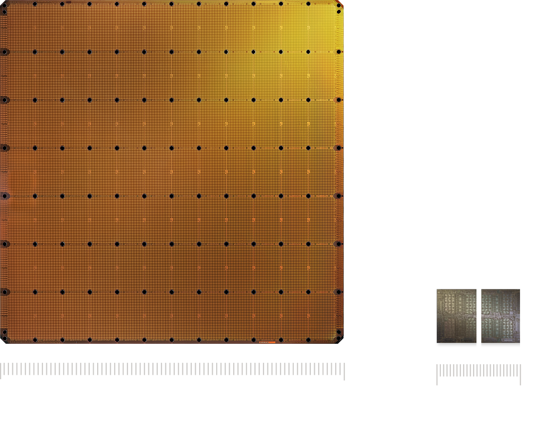
WSE-3 occupies an entire 300 mm wafer, 46,225 square millimeters, 57× larger than an H100, with 4 trillion transistors, 900,000 cores, 44 GB of on-chip SRAM, and 21 PB/s on-chip memory bandwidth. It solves engineering problems that were considered unsolvable for decades — wafer-level yield (via redundancy + interconnect rerouting), power delivery (liquid cooling + high-density power grid), thermals (on-chip liquid cooling channels).
But Cerebras’s key insight isn’t about “faster compute”; it’s that inter-chip communication is 100× slower than on-chip communication:
- Traditional GPU cluster: split Llama 70B across 8 H100s, interconnect via NVLink (900 GB/s) — still an order of magnitude slower than single-chip SRAM (~10 TB/s)
- Cerebras WSE-3: the entire 70B model lives on a single “chip” — no inter-chip communication at all
That’s why Cerebras hits ~2,000 tok/s on low-latency inference — not because per-unit compute is faster than the GPU, but because it eliminates the big block of time spent “waiting for data to arrive from a neighboring chip.”
But Cerebras is still “general parallelism” — the compute units inside the chip can run any PyTorch operator, not locked to Transformers. The OpenAI contract signed in early 2026 (over $10B, 750 megawatts) was specifically about this point — not wanting to be locked into a specific architecture, while needing ultra-low latency. This is Cerebras’s biggest difference from the Transformer-specific chips that follow.
Why Cerebras Sits on the “General” Side — process innovation vs architectural specialization
An easy trap is to classify Cerebras as a “specialized ASIC” — because it “doesn’t look like a traditional chip.” But Cerebras’s innovation dimension lies entirely off the “specialization” axis:
| Dimension | NVIDIA GPU | Cerebras WSE-3 | TPU / Groq / d-Matrix… |
|---|---|---|---|
| Architectural innovation | General parallel + heterogeneous accelerators | Wafer-scale integration (physical form) | Cut general portion, specialize for matmul |
| What it can run | Any operator | Any operator | Matmul + mainstream NN operators |
| Problem solved | Compute uplift | Inter-chip communication bottleneck | Energy waste in general-purpose hardware |
Cerebras’s physical-form innovation is orthogonal to “specialization” — you could absolutely build a “wafer-scale + in-memory compute” chip that eliminates both inter-chip communication and the SRAM-to-compute-unit shuttling within a die. It’s just engineering-prohibitively difficult; no one can do two radical things simultaneously. Cerebras picked the wafer-scale side, d-Matrix picked the in-memory side, and each is digging into their respective side first.
So the two gradients on the far left aren’t a “ranking comparison”; they’re “different bottlenecks each have their own attackers” — NVIDIA attacks “extreme single-card,” Cerebras attacks “inter-chip communication.”
Systolic Arrays — Cutting Away the General Part — Google TPU
Starting from this gradient, we enter actual “specialization” — the TPU extracts the Tensor Core from inside the GPU and scales it up, cutting away CUDA Cores and other general computation parts, with all silicon area devoted to matmul.
The Systolic Array Circuit — a “scaled-up” Tensor Core
The core idea of the systolic array, proposed by H.T. Kung in 1979, is: data flows through a fixed array of processing elements (PEs) like a heartbeat, with each PE doing one multiply-add and passing the result to a neighbor or accumulating locally. This means:
- Once data enters the array, it almost never needs to access main memory again
- Control circuits only need to manage the “clock,” not “scheduling,” so circuit overhead is minimal
- Within the same silicon budget, you can fit several times more multiply-add units than a GPU
But the systolic array has a fatal weakness — it only suits regular matrix multiplies. As soon as computation involves irregular memory access (sparse attention, dynamic shapes, complex control flow), the systolic array runs poorly. That’s why TPUs run Transformer inference smoothly but struggle with state-space models like Mamba.
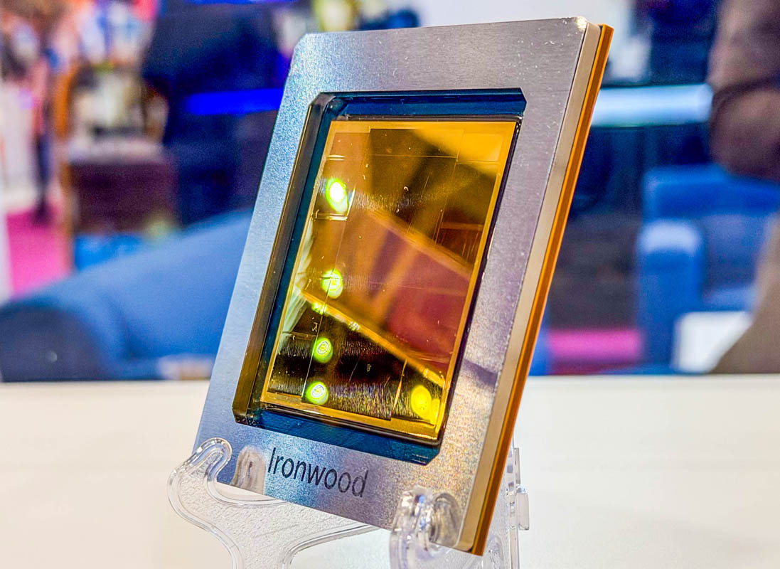
The seventh-generation Ironwood pushed this “specialization” to the point where Google itself felt the need to split — they released TPU 8t (training-specific) + TPU 8i (inference-specific), two different chips. The TPU 8i pairs 288 GB HBM with 384 MB on-chip SRAM, optimized specifically for MoE and long-context models. This means even Google has acknowledged “training and inference need different hardware” — something unimaginable in the TPU v3 era of 2018.
TPU 8t / 8i Training-Inference Split — first acknowledgment that the two ends need different hardware
Why split? Because the workload shapes for training and inference are fundamentally different:
- Training: large batches (hundreds to thousands), aims for peak throughput, latency-insensitive, requires backpropagation (gradient computation) and optimizer state. Each step needs memory 4-7× the parameter size.
- Inference: small batches (1-16), aims for low latency, no backpropagation needed, memory only needs to hold weights + KV cache.
Doing both tasks on the same chip leads to severe waste — a training chip doing inference has most of its circuitry idle; an inference chip doing training can’t sustain backpropagation. TPU 8t / 8i is Google’s first physical split of these two workloads — the inference chip is extremely optimized for “single-stream low latency + long-context KV cache,” while the training chip is extremely optimized for “cluster coordination + large-batch throughput.”
This has industry-level signal value: specialization has fractionated to the precision of “the same operator needs different hardware under different workloads.” We’ll see later that Groq, d-Matrix, and Etched all only do inference — training simply doesn’t show up on the specialization spectrum, because algorithms are still evolving, and no one dares to tape out for a specific training flow.
Same-Path Players — AWS Trainium · Huawei Ascend · Meta MTIA
Google isn’t alone on the systolic array path — almost every cloud provider has gone this route:
- AWS Trainium / Inferentia: more explicitly split (Trainium for training, Inferentia for inference), with 1.4 million Trainium units deployed. Anthropic’s Claude runs on over 1 million Trainium2s, with a 10-year commitment of over $100B invested into AWS to lock in up to 5 GW of capacity.
- Huawei Ascend: the Da Vinci architecture’s 3D Cube matrix compute unit is essentially a systolic array. The Q1 2026 Ascend 950PR features self-developed HBM; “super-node” interconnects build Atlas 950/960 SuperPoD clusters, and the 8192-card cluster compute already exceeds NVIDIA’s NVL576 roadmap.
- Meta MTIA: internal ASIC developed in collaboration with Broadcom, primarily for Meta’s own recommendation, ads, and Llama training.
- Microsoft Maia: internal AI chip developed in collaboration with OpenAI; second generation released in early 2025.
Put these together and an industry-level pattern emerges — every company with “its own cloud + sufficient model scale” is doing a systolic array ASIC. The reason is simple: bypass NVIDIA’s high margins (40-70%) and internalize that profit. The moat of this path isn’t technology — systolic arrays aren’t that mysterious — it’s “own-cloud internal shipment volume sufficient to amortize tape-out cost.” That’s why independent systolic-array companies have a hard time surviving, but cloud providers doing this make money.
Compile-Time Frozen Scheduling — Groq LPU
One gradient to the right, we arrive at the Groq LPU (Language Processing Unit) — on top of the systolic array’s “cut away the general part,” it cuts away another thing: runtime scheduling.
Deterministic Dataflow — the price of no dynamic scheduling
Groq founder Jonathan Ross was a co-author of the original Google TPU. He felt that the TPU wasn’t extreme enough — although the TPU cut away CUDA Cores, it retained the traditional CPU model of “execute by instruction,” with runtime complexity from warp scheduling, cache hierarchy, branch handling, etc. Ross’s insight: for neural network inference, all of that “dynamic behavior” is waste.
The Groq LPU’s core architecture is called the “statically scheduled Tensor Streaming Processor” (TSP):
- At compile time, exactly where every token and every clock cycle of data flows is fully planned
- At runtime there’s no scheduling overhead, no cache misses, no branch mispredictions
- The entire pipeline is like a precision loom — every clock cycle, every gear position is deterministic
This “determinism” yields three direct benefits:
- Extremely low latency: Llama-3 8B runs at 1,345 tokens/s, several to over ten times the GPU
- Extremely high energy efficiency: what’s saved isn’t just compute energy, but scheduling-circuit energy too
- Predictable throughput: no “this frame suddenly stalls for 100ms” GPU-common phenomena
The price is: long compile time, expensive model switches. Changing a model is like redesigning the loom. But Groq solved this elegantly — treat compilation as a one-time investment, then expose compiled models as a “service” (the GroqCloud API). Developers pay per token and don’t have to run compilation themselves.
All-On-Chip SRAM — the no-HBM design philosophy
The Groq LPU has another counterintuitive design choice: no HBM at all.
Each LPU has 230 MB of SRAM, with no HBM and no DRAM. SRAM capacity is small, but bandwidth is several times HBM’s, and energy consumption is an order of magnitude lower. The problem is 230 MB per chip can’t hold a large model — a Llama 70B requires 140 GB (FP16). Groq’s answer: form clusters. Hundreds of LPUs use proprietary high-speed interconnect to form a cluster, each LPU holding a slice of the model.
This brings us back to the same “inter-chip communication” problem Cerebras solves — Groq’s answer is “self-developed ultra-low-latency interconnect,” not as general as NVLink, but enough to make hundreds of LPUs work as a single unit.
Not depending on HBM is a hidden advantage of Groq. Against the backdrop of HBM shortages in 2024-2026 (Samsung / SK Hynix / Micron capacity all locked up by NVIDIA), no HBM = no queue. Groq can scale capacity independently, one of the hardware reasons it could ramp quickly in 2024-2025.
2 Million Developers + NVIDIA’s $20B Endorsement — the strongest commercial validation
Groq’s commercial progress is the fastest on the spectrum:
- 2025 revenue projected at 1.2B, 2027 $1.9B
- GroqCloud serves over 2 million developers, with 75% of Fortune 100 companies having an account
- August 2024 Series D 2.8B), September 2025 another 6.9B), plus a $1.5B Saudi commitment
But the most significant event was the NVIDIA-Groq deal in early 2026: NVIDIA struck an approximately $20B agreement with Groq, licensing Groq’s AI inference technology and absorbing several Groq executives into NVIDIA. The implication is crystal clear — NVIDIA itself wants Groq’s path capabilities but doesn’t want to compete, so it chose “acquire the technology + recruit the people” instead of “compete head-on.”
This is the one time NVIDIA has formally acknowledged the value of a non-GPU path across the entire spectrum. It means the “compile-time frozen + all-on-chip SRAM” path that Groq represents has an advantage on low-latency inference that no GPU modification can match — a judgment NVIDIA cast its $20B vote for.
Storage and Compute Physically Fused — d-Matrix digital in-memory computing
The middle gradient of the spectrum looks “counterintuitive” — let storage units do compute themselves, or physically fuse compute units with storage units. This is the digital in-memory computing (DIMC) path that d-Matrix takes.
The Memory Wall — moving data costs 10× more than computing
To understand why anyone would do this, you need to understand a fundamental waste in traditional chips — the “memory wall” problem:
A GPU running Llama 70B inference, for every token generated, in theory has to read all 70 billion weight parameters from HBM through the compute units once. The energy of shuttling that data is more than 10× the multiply-add operation itself. Most of the H100’s silicon budget is spent solving “how to move weight data to compute units faster” — HBM3, L2 cache, TMA async transfer, layer upon layer of optimization — but it’s all “mitigation,” not “cure.”
d-Matrix’s core reframe: since every inference has to read the weights, why not just compute them where they’re stored?
Stuffing Multipliers Next to SRAM — a chiplet grid
What d-Matrix concretely does is digital in-memory computing (DIMC) — rather than letting storage units do compute themselves, it places the compute unit tightly adjacent to the storage array. The two are interleaved physically within a chiplet, weights permanently resident, no repeated shuttling needed.
Versus “analog in-memory computing” (the path that Mythic and EnCharge AI take) — analog schemes attempt to encode weights directly as conductance values of devices like ReRAM, using Ohm’s law + Kirchhoff’s current law to physically perform matrix multiply as current flows through the array. Energy efficiency could theoretically be an order of magnitude higher, but the engineering difficulties are enormous (ADCs are too expensive, write precision is poor, temperature drift, finite lifespan).
d-Matrix actually tried the analog path early on (the Nighthawk concept chip in 2020), but quickly gave up — “putting an ADC on every bitline is too hard.” Ultimately they went with digital IMC (DIMC), sacrificing some of analog’s peak efficiency in exchange for engineering feasibility + controllable precision. This is a very honest call.
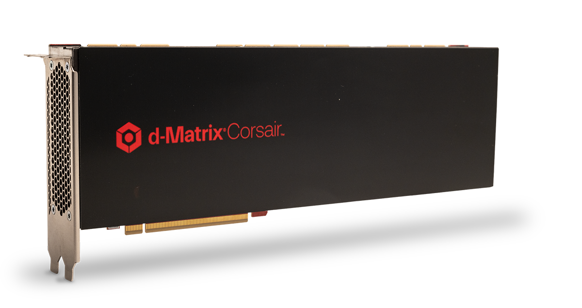
Engineering-wise, the d-Matrix Corsair’s concrete design:
- Based on 6nm Nighthawk + Jayhawk II chiplets
- Each Nighthawk integrates 4 neural cores + a RISC-V CPU
- Chiplet packaging, standard PCIe Gen5 full-length full-height card
- Compared to GPU solutions: 10× performance, 3× cost reduction, 3-5× energy efficiency uplift
- Single card hits 30,000 tokens/s on Llama 70B with 2 ms per-token latency
d-Matrix’s next-generation roadmap is even more aggressive — partnering with Alchip to build the world’s first 3D-stacked DRAM solution, 3DIMC, debuting on Corsair’s successor Raptor inference accelerator, claimed to be 10× faster than HBM4 solutions. This pushes “in-memory” thinking further from SRAM to DRAM.
Intra-Layer Parallel + Inter-Layer Pipelined — fire simultaneously · advance in pipeline
DIMC and GPUs have a subtle but key difference in “how computation happens” — intra-layer fires simultaneously, inter-layer advances in pipeline:
This is fundamentally different from Google TPU’s systolic array:
- Systolic array (TPU): computing one layer takes hundreds of clock cycles — data moves stepwise between PEs like a heartbeat, and you have to wait for data to flow through the entire array
- DIMC (d-Matrix): computing one layer takes a few clock cycles — inputs are broadcast to all PEs, computed simultaneously, output simultaneously
The “flow” in a systolic array is fine-grained — data really is moving step by step between cells. In-memory computing is coarser-grained — data flows between layers, but within a layer it’s instantaneous. Inter-layer is like a conveyor belt, one layer after the next; intra-layer is like an explosion, the entire layer completing in an instant.
Time Multiplexing When Model > Hardware — slicing the model
DIMC has an implicit limit: the chip’s hardware capacity determines how much of the model can fit. A single Corsair card has 2 GB high-performance memory + 256 GB capacity memory, which can’t hold all layers of a Llama 70B resident simultaneously.
The practical engineering approach is “time multiplexing”:
- Slice the model into several “segments”
- Write the first segment into hardware, run it; swap weights to the next segment, continue
- Intermediate results buffered in capacity memory
This sounds like a regression back to GPU behavior — the GPU also runs infinitely many layers with finite compute units. But the key difference is shuttle frequency:
- GPU: every token rereads all weights (weights in HBM)
- DIMC: once a set of layers is written in, it can process many tokens before swapping to the next set
DIMC’s core advantage isn’t “completely eliminate weight shuttling,” but reduce shuttle frequency from “once per token” to “once per batch” or less. This is how d-Matrix can deliver several-to-10× GPU energy advantage while preserving the flexibility of “any Transformer.”
Commercially, d-Matrix is the most mature in the middle of this spectrum:
- Launched Corsair end of 2024, general availability Q2 2025
- Closed 2B, oversubscribed), backed by Microsoft M12, Qatar Investment Authority (QIA), Temasek
- Co-released SquadRack open standard reference architecture with Arista, Broadcom, Supermicro
- Acquired GigaIO’s data center business in April 2026, extending to rack-scale solutions
The Transformer Operator Graph Etched Into Silicon — Etched Sohu
Pushing one more gradient to the right of the spectrum, we arrive at an even more radical design — burn the entire Transformer operator graph into a hardwired circuit. Etched Sohu represents this path.
Etching the Operator Graph Into Dedicated Circuits — cutting away all non-Transformer hardware
Etched’s core reframe differs from every previous path — since the Transformer has won, why preserve hardware for “other architectures that might appear in the future”?
Concrete approach:
- Burn all standard Transformer operators (matmul, softmax, LayerNorm, RoPE positional encoding, KV cache management, etc.) into hardwired circuits
- Retain no support for CNNs, RNNs, state-space models (Mamba/RWKV), etc.
- Weights are still loaded via software (unlike Taalas which etches weights into silicon too) — so it can run any Transformer model
This “trimming” is highly aggressive. By removing all hardware required by non-Transformer neural networks, Etched fits more Transformer-specific compute into the same silicon — on the same TSMC 4nm process, the Sohu’s “effective Transformer compute” is an order of magnitude higher than the H100.
500K tok/s on Llama 70B with 8 Cards — 20× an H100 server
Etched’s performance numbers are stunning:
- An 8-card Sohu server hits over 500,000 tokens/s on Llama 70B
- An H100 server on the same model is around 23,000 tokens/s — Sohu is 20× faster
- A B200 server is around 45,000 tokens/s — Sohu still 10× faster
- Claimed: one 8-card Sohu replaces 160 H100s
The number is large enough to invite skepticism, but the underlying logic holds up: roughly 70-80% of an H100’s silicon area is spent on things “not serving Transformer inference” (the general portion of CUDA Cores, RT Cores, graphics-related circuits, various scheduling logic). Sohu cuts all of that, lifting the share of silicon serving pure Transformer inference from ~20% to near 100% — 5× more compute is reasonable, plus the energy efficiency advantage of specialization makes a combined 10-20× not absurd.
Risk — if Transformer is replaced, the chip goes to zero
Sohu’s risk is crystal clear: if the Transformer is replaced by a fundamentally different architecture within 5-7 years, every Sohu chip instantly goes to zero.
Potential threats:
- Mamba / state-space models: more efficient than Transformers in long-context scenarios, with substantial academic progress in 2024-2025.
- MoE extreme sparsification: although MoE is still in the Transformer family, some aggressive sparse expert schemes require hardware-supported dynamic routing — whether Sohu supports it depends on the specific implementation.
- Next-generation “attention replacements”: Linear Attention, Retentive Network, xLSTM, etc., all challenging standard attention.
But Etched’s own bet is that the Transformer has won too completely. GPT/Claude/Gemini/Qwen/DeepSeek/Llama are all Transformer variants, hundreds of billions of training investment is all bet on this — the “transition cost” of changing architectures is too high for the industry to push it proactively. This is a high-beta bet: double the valuation if right, zero if wrong.
Commercially, Etched is valued at around $800M, shipping to early customers from 2024. Its lower valuation than d-Matrix isn’t because the tech is worse, but because deeper specialization → more risk → larger market discount. This is the general pattern we’ll return to — valuations correspond precisely to position on the spectrum.
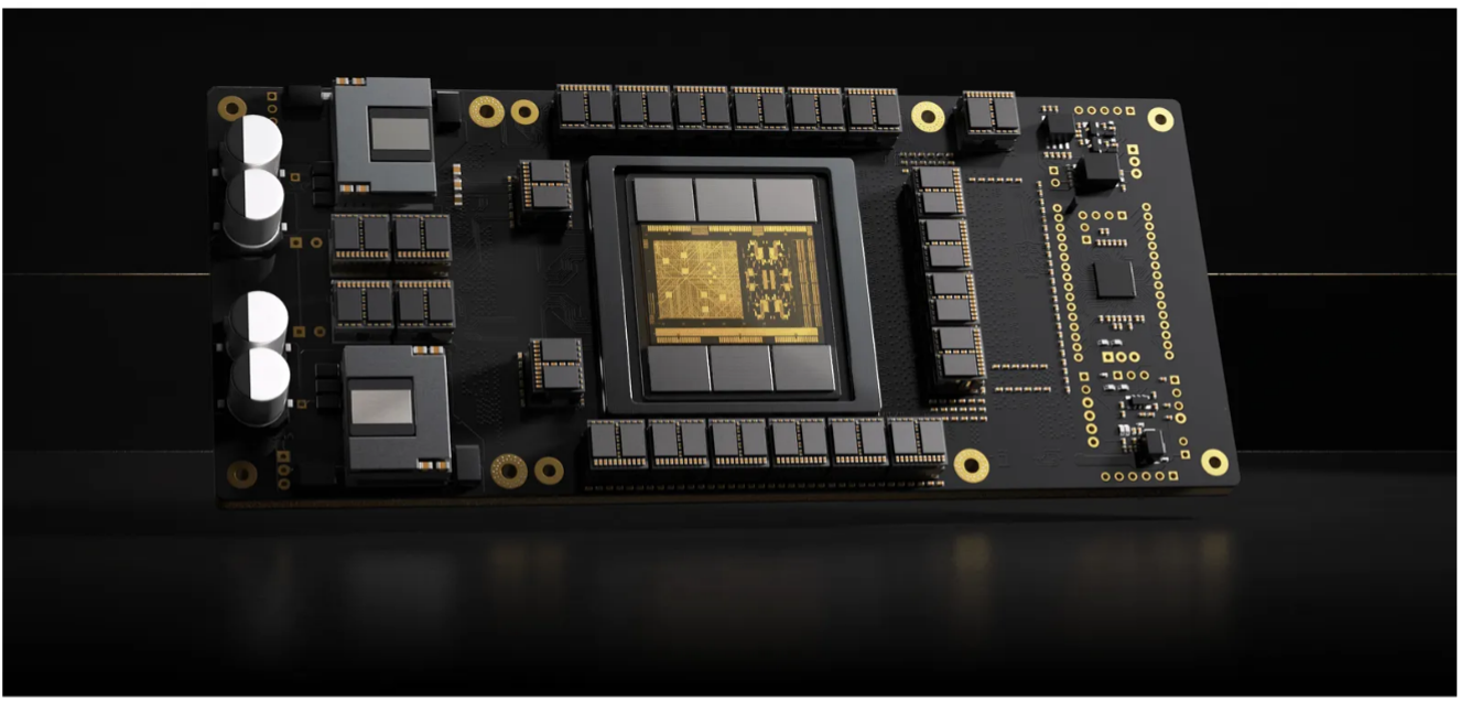
Physically Casting Weights Into Silicon — Taalas HC1
The rightmost gradient of the spectrum is the true “nuclear option” — not only is the architecture etched in stone, the model’s weights are also physically cast into the silicon. This is the path Taalas takes.
The Structured ASIC Path — change 2 mask layers · tape out in 2 months
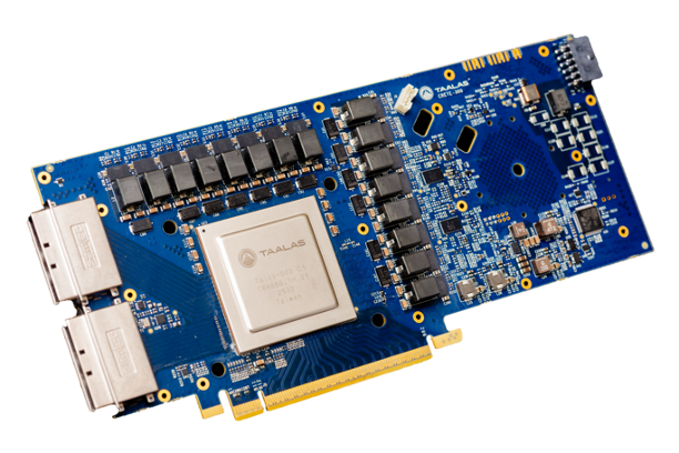
Taalas (Canadian company, emerged from stealth in February 2026 with $169M raised), core approach:
- Physically encode the weights of a specific LLM into the chip’s silicon structure — much like a CD-ROM, game cartridge, or printed book
- No HBM or external weight storage required at all — memory and compute logic combined on a single chip at DRAM-class density
- Borrowing the “structured ASIC” idea from the 2000s — using gate arrays and hardened IP modules, only changing the interconnect layer to adapt to specific workloads
“Change only 2 mask layers” is Taalas’s key engineering breakthrough. A chip typically has 10+ mask layers, and a normal tape-out redoes all of them. Taalas builds all reusable circuits as a “base platform,” and only changes 2 interconnect mask layers for a specific model — this brings tape-out cost and time down by ~10×, going from receiving a new model to producing hardware in just 2 months.
The HC1 first-product specs:
- TSMC 6nm, 815 mm² (close to the H100’s size), ~53 billion transistors
- No HBM stack, no 3D stacking, no water cooling
- ~250 W power, with 10 HC1 cards per server totaling 2.5 kW, deployable in a standard air-cooled rack
- The core mechanism likely involves analog computing techniques — resistor-network weight encoding + log-domain arithmetic, enabling single-transistor multiplication
Single Chip, Single Model, 17,000 tok/s — 28× B200
Taalas’s performance on the “single model” benchmark is staggering:
- HC1 physically casts Llama 3.1 8B into silicon — 17,000 tokens/s per user
- Vs NVIDIA B200 on the same model ~594 tokens/s — 28× advantage
- Vs Cerebras WSE-3 ~1,981 tokens/s — 8× advantage
- Vs Groq LPU ~600 tokens/s — 28× advantage
- Cost per million tokens 0.75 cents — 20× lower than the GPU path
This is the most extreme single-point performance on the entire spectrum. But the cost is clear — this single chip can only run Llama 3.1 8B, not Llama 3.2, not Qwen 2.5, and certainly not any non-8B model.
Hedging Model Iteration With “Fast Tape-Out” — 30 tape-outs supports R1-671B
Taalas’s business model is unique — using “fast tape-out” to hedge “model iteration”:
- Customer picks a specific model to deploy (say, DeepSeek R1-671B)
- Taalas tapes out a few dozen chips for this model in 2 months
- Assuming the model is in service for 1-2 years with sufficient deployment volume, the unit economics work
- When the model changes, the customer either re-tapes (another 2-month wait) or swaps chips
Taalas itself claims 30 tape-outs can support a large model like DeepSeek R1-671B (since 671B is too large, it has to be distributed across many chips, each holding a small slice of weights). This is essentially an “anti-Moore’s law” product strategy — making money not from process advancement but from the engineering capability to “quickly adapt to model changes.”
The biggest risks on Taalas’s path:
- Model lifecycle vs tape-out cycle race. If a hit model loses relevance in 6 months, even Taalas’s 8-week tape-out can’t keep up. This requires commercial customers to make long-term model-choice commitments.
- Hardcoding creates new technical debt. After shipment, the AI portion can’t be upgraded; customers expecting software-update cycles will strongly resist — data center customers typically expect hardware to be in service 5-7 years.
- Customer lock-in. The Taalas chip is usable only for the specific model; customers can’t run other models, leaving them with minimal bargaining power.
But Taalas’s existence itself proves — the industry is willing to put physical capital into the most extreme “specialization” direction. Even if most customers ultimately don’t choose this path, just the existence of the option puts back-pressure on every more-general scheme — d-Matrix and Etched must demonstrate their flexibility premium is worth the several-times speed gap.
The Photonic Path Splits — compute paused · interconnect explodes
That covers the seven main gradients. But one parallel path deserves a dedicated discussion — photonic chips. It’s not on the main spectrum, but it has important intersections with it: photonics is blocked at “compute” by the diffraction limit, but has scaled at “interconnect.”
Photonic Computing’s Physical Advantages — multiply-add natural · energy efficient · distance independent
The core insight of photonic computing is simple — matrix multiplication is essentially “multiply” and “add,” and light naturally does both:
- Multiplication: a beam of light passing through a medium with 50% transmittance has its intensity automatically multiplied by 0.5. If a Mach-Zehnder interferometer (MZI) is used to precisely control transmittance, light intensity can be multiplied by any weight value.
- Addition: two beams of light shining on the same detector produce a total intensity = sum of both. Physical superposition of light = addition.
- Parallelism: light of different wavelengths (colors) propagates in the same medium without interference. Running 16 colors of light through the same optical path is like 16 independent computations completed simultaneously — something electrons can’t do at all.
This sounds wonderful. The truly attractive physical advantages of photonic computing:
- Extreme energy efficiency: Q.ANT NPU runs workloads at 30 W, vs GPU 700-1000 W — an order of magnitude lower energy for the same matmul task
- Extreme speed: light travels through silicon waveguides at ~75,000 km/s, with near-instantaneous signal settling
- Natural parallelism: WDM lets one optical path simultaneously run a dozen-plus independent computations
- Almost no heat: heat is concentrated at the electro-optic / opto-electronic conversions at both ends; almost no heat in the middle
- Immune to EMI: light is electrically neutral, with several beams in the same medium not crosstalking
The Diffraction Limit — why photonics can never reach nanoscale density
But photonic computing has a fundamental physical bottleneck — the diffraction limit:
Photonic device sizes cannot be smaller than half the wavelength of the light — that’s a physical law, called the diffraction limit. Mainstream data center optical communication uses 1310 nm or 1550 nm infrared light, with a diffraction limit of ~700 nm (half a micron). In practical engineering, after accounting for manufacturing tolerances, loss management, and wavelength drift, photonic devices must be much larger:
| Photonic Device | Typical Size | vs Electronic |
|---|---|---|
| Single optical waveguide (one guide line) | 500 nm wide, 1-2 μm spacing | Single transistor 20-30 nm |
| Microring modulator (MRM) | 5-10 μm diameter | - |
| Mach-Zehnder modulator (MZM) | 100 μm to several mm long | - |
| Single MZI compute unit | tens to hundreds of μm | Single Tensor Core ~10 μm |
The density gap is ~200-500×. This produces a direct engineering reality — on an H100-sized silicon die (800 mm²), electrons can fit dozens of 1024×1024 matrix multipliers, while photons can fit a maximum matrix multiplier of about 128×128.
Worse — this gap is dictated by physics, and process improvements can’t solve it. Even pushing photonic processes from today’s 45 nm/90 nm to 3 nm, photonic device density barely improves (since it’s not process-limited, it’s wavelength-limited). Unless you use X-ray wavelengths (a few nanometers), but those energies would destroy silicon itself.
Photonic Computing — still in the coprocessor stage
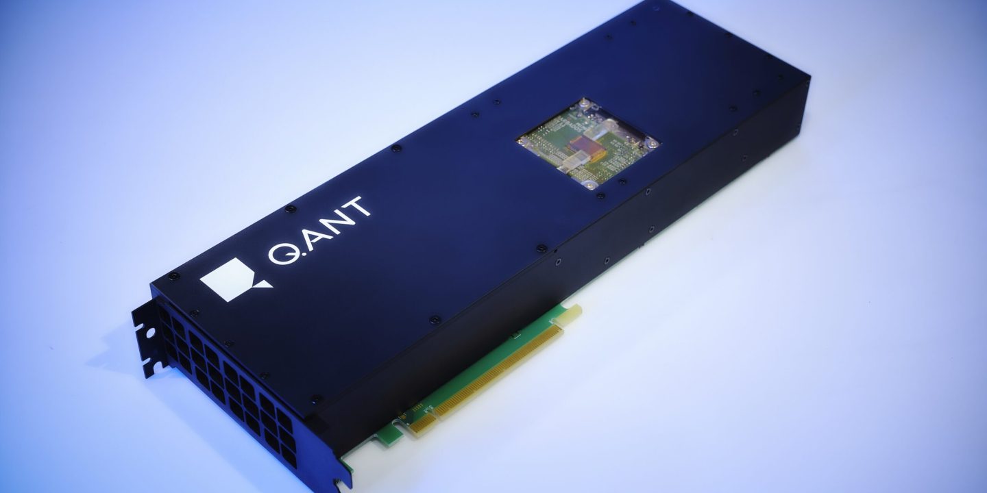
The actual state of photonic computing today — coprocessor, not replacement. Q.ANT is the most demo-worthy representative of this path:
- NPU already deployed at the Leibniz Supercomputing Center (LRZ) in Munich, in use as a production HPC coprocessor
- 6× more energy-efficient than GPUs on real workloads
- Achieved 16-bit floating point precision — the key threshold for AI training and inference
- NPU 2 is orderable, shipping to customers from H1 2026 as a standard 19-inch server
But photonic computing’s fundamental shortcomings remain unsolved:
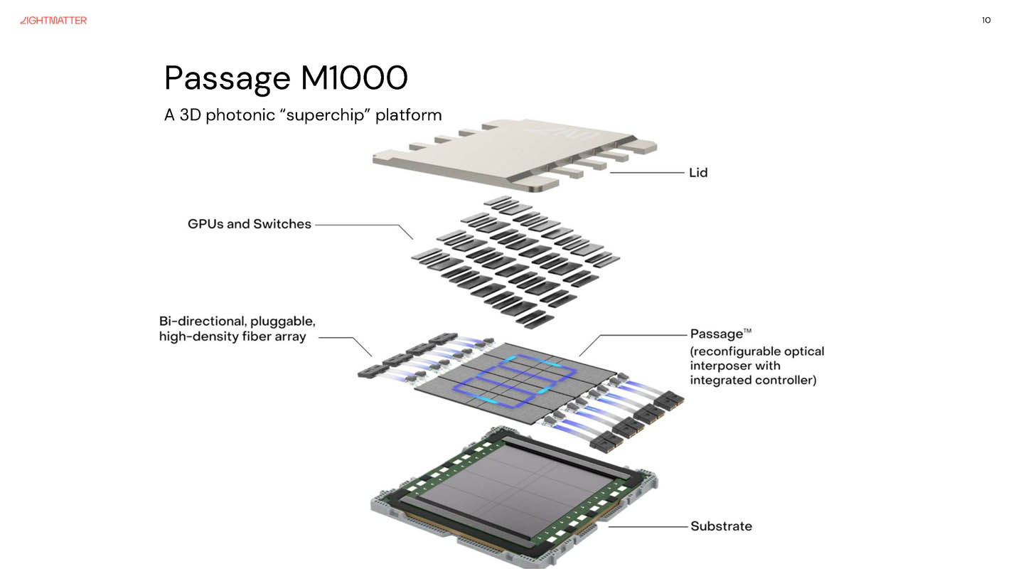
- Physical size: at equivalent compute, photonic chips are 30-100× larger than GPUs. Lightmatter’s Envise (photonic compute) was essentially “downgraded” by the company for this reason — Lightmatter now leads with Passage (photonic interconnect), with Envise as a research project
- Limited precision: analog computing inherently has noise; 16-bit is a huge breakthrough but doesn’t match GPU FP32 reproducibility
- Low absolute compute: the most advanced photonic processor in a 2025 Nature paper hits 65.5 TOPS (16-bit), only 3% of an H100 (INT8 ~2000 TOPS)
So the best near-term (within 5 years) positioning for photonic computing is coprocessor — let the CPU/GPU do what it’s good at (control, scheduling, nonlinear ops), and offload matmul to photonics. This is Q.ANT’s actual deployment model.
Photonic Interconnect — GPU cluster scaling already shipping
The other fate of photonics is completely different — photonic interconnect has scaled to commercial use. It solves not the compute bottleneck but the “interconnect wall” — GPU clusters growing larger while electrical interconnect bandwidth can’t keep up.
Key advantages of photonic interconnect:
- Extreme bandwidth density: a single fiber can run dozens of different wavelengths simultaneously via WDM — for the same physical footprint, optical bandwidth is dozens of times copper’s
- Distance independent: copper lines attenuate more the longer they run; fiber is nearly distance-independent. For hundreds-of-meters of rack interconnect in an AI data center, light is the only choice
- Better energy efficiency: per-bit energy ~4-5 pJ/bit for light vs ~7-15 pJ/bit for copper SerDes — roughly 2-3× advantage
Why has the AI era forced out photonic interconnect? The data is unambiguous — model parameters have grown 240× in 3 years, cluster scale 10×, but electrical interconnect bandwidth only 2×. The gap widens; copper at 224 Gbps is near its physical limit (faster brings severe crosstalk). Light has to step in.
Commercial progress is fast:
- Lightmatter: 850M raised; Passage M1000 shipping, L200 co-packaged product launches 2026
- Ayar Labs: valuation over $1B, backed by AMD Ventures, Intel Capital, NVIDIA, 3M Ventures
- Celestial AI: acquired by Marvell for $3.25B at end of 2025 — strong exit signal
- NVIDIA itself launched Quantum-X and Spectrum-X photonic platforms in 2025; Quantum-X switches shipped from late 2025
When NVIDIA itself enters photonic interconnect, this path is no longer an “alternative” — it’s the necessary path for AI cluster scaling.
Energy Comparison — 4-5 pJ/bit vs 7-15 pJ/bit
Putting the key metrics of photonic and electrical interconnect side by side:
| Dimension | Electrical (copper SerDes) | Photonic (silicon photonics CPO) |
|---|---|---|
| Current state-of-the-art per-bit energy | 7-15 pJ/bit | 4-5 pJ/bit |
| Best lab record | 1.41 pJ/bit (224 Gb/s, 2022) | 0.7 pJ/bit (112 GBaud, 2023) |
| Bandwidth ceiling | ~224 Gbps/lane | dozens of wavelengths multiplexed |
| Distance attenuation | severe | nearly none |
| Process maturity | extremely mature | GF 45nm/90nm volume |
| Per-die integration ceiling | tens of Tbps | >100 Tbps (per package) |
The energy advantage of photonic interconnect isn’t “crushing” (only 2-3×); its real edge is bandwidth density + distance independence.
Synthesis — the flexibility-vs-efficiency tradeoff spectrum
Having walked the seven gradients + photonic branch, we can put all the data together for an overall synthesis.
Speed Across the Seven Gradients — measured Llama 70B / 8B data
Putting the measured throughput data for every product on the spectrum together:
| Path | Representative Product | Status | Llama 70B (8 cards) | Llama 70B (single stream) | Physical Implementation |
|---|---|---|---|---|---|
| General GPU | NVIDIA H100 | scaled | ~23,000 tok/s | ~50 tok/s | CUDA + Tensor Core |
| General GPU | NVIDIA H200 | scaled | ~31,712 tok/s | ~70 tok/s | same + HBM3e |
| General GPU | NVIDIA B200 | scaled | ~45,000 tok/s | ~120 tok/s | Blackwell |
| Wafer-scale | Cerebras WSE-3 | commercial | - | ~2,000 tok/s | entire wafer |
| Static dataflow | Groq LPU | scaled | - | ~600 tok/s | compile-time frozen |
| Digital in-memory | d-Matrix Corsair | shipping | - | ~500 tok/s | digital in-memory compute |
| Transformer ASIC | Etched Sohu | early customers | >500,000 tok/s | ~60,000 tok/s | operator graph etched |
| Model etched | Taalas HC1 | just released | - | 17,000 tok/s (L8B) | weights cast into silicon |
Note: these numbers come from vendor public materials and third-party reports; measurement conditions aren’t fully comparable across them — but the order-of-magnitude relationships are clear. Each step right on the spectrum brings a 3-10× speed gain, with a cumulative range approaching 1000×.
Valuation Maps Precisely to Spectrum Position — more specialized = lower valuation
Stacking the valuations of every company on the spectrum produces a remarkably clean gradient:
| Company | Path | Valuation | Distance from most specialized |
|---|---|---|---|
| NVIDIA | GPU (most general) | $4T+ | far left |
| Cerebras | wafer-scale | ~$49B (2026/5 IPO valuation) | scaled |
| Groq | static dataflow | ~$6.9B | $20B NVIDIA endorsement |
| d-Matrix | digital in-memory | ~275M) | Series C oversubscribed |
| Etched | Transformer ASIC | ~$800M | shipping to early customers |
| Taalas | model etched | <$500M (estimated) | just released, $169M raised |
This isn’t coincidence — it’s the market’s precise pricing of “specialization risk.” The more specialized the scheme, the more concern about hardware going to zero if model architectures change in the future — so the larger the discount the market applies. NVIDIA is worth $4T partly because of its “generality premium” — no matter how AI evolves, GPUs never go to zero.
Conversely, it makes sense — Taalas’s low valuation isn’t because the tech is bad, but because the downside risk of “betting on one model” is inherently large.
The Steady-State Landscape Over the Next 3-5 Years — training / inference / interconnect, three markets
The entire AI inference chip landscape over the next 3-5 years roughly settles like this:
Training market (70-30 split) — basically settled:
- NVIDIA (~70%): generality is the core requirement for training, since algorithms are still evolving
- Google TPU (~20%): own-cloud + Anthropic and other large customer internal absorption
- AWS Trainium etc. (~10%): cloud provider in-house use cases
Inference market (splitting into several sub-tracks) — this is the truly diverse part:
- Large-scale cloud inference services → GPU + TPU + Trainium (NVIDIA still dominant but share declining)
- Extreme low-latency inference (agents, dialogue) → Groq + Cerebras
- Data center scale cost reduction → d-Matrix (digital in-memory)
- Single hit-model deployment (edge API, customer service) → Etched + Taalas
- Edge inference (phones, cars, IoT) → Apple ANE, Qualcomm Hexagon, Horizon Robotics Journey, other NPUs
Interconnect market (newly emerging sub-category) — photonic interconnect becomes a “must”:
- Lightmatter Passage series
- Marvell-Celestial (post-acquisition integration)
- Ayar Labs optical I/O
- NVIDIA’s own Quantum-X / Spectrum-X photonic switches
This is an unusual industry window — no one displaces anyone, instead different solutions eat different sub-segments. This is completely different from the past decade of “GPU rules all,” and it’s what makes this wave of AI inference chip startups genuinely interesting.
The last variable worth watching — will large-model architectures change? If the Transformer is replaced by Mamba, xLSTM, or some entirely new architecture within 5-7 years, schemes like Etched and Taalas that “bet on one architecture” go to zero; d-Matrix and Groq take a hit but can still survive; Cerebras, TPU, and NVIDIA are almost unaffected. The valuation gradient’s core logic is exactly the market’s pricing of this risk.
If you believe “the Transformer has at least 5 years left” — Etched / Taalas bets are good trades. If you think “a new architecture is inevitable within 3 years” — the money should be on the left side of the spectrum. This is the most important decision framework the spectrum offers investors.
References — company materials · industry reports · technical papers
Company Websites and Official Announcements
- NVIDIA — H100 product page, DGX B200, GTC 2024 / 2025 keynotes, Blackwell / Rubin architecture white papers
- Cerebras — WSE-3 product page, 2026 IPO prospectus (S-1), OpenAI $10B contract announcement
- Google Cloud — Google Cloud Blog TPU v7 Ironwood announcement (2025), TPU 8t / 8i training-inference split technical blog
- Groq — Groq site, LPU TSP architecture white paper, NVIDIA-Groq $20B partnership announcement (2026)
- d-Matrix — Corsair product page, SquadRack open standard reference architecture, GigaIO acquisition announcement
- Etched — Etched site, Sohu announcement, Llama 70B 500K tok/s performance data
- Taalas — “The Path to Ubiquitous AI” (2026/2), HC1 product overview
- Lightmatter — Lightmatter site, Passage M1000 / L200 white papers, Hot Chips 2025 talk
- Q.ANT — Q.ANT site, NPU second-generation product materials (2025), Leibniz supercomputing center deployment case
Industry Reports and News
- Deloitte — 2026 AI workload forecast (inference ~2/3, 2027 expected 80%)
- McKinsey — AI compute market report (compute spend vs inference share)
- ServeTheHome — Google TPU v7 Ironwood report, Lightmatter Passage at Hot Chips 2025 report, Cerebras WSE-3 review
- SemiAnalysis — Dylan Patel’s deep analysis of inference chips, ASIC vs GPU economic modeling
- The Information / Bloomberg — NVIDIA-Groq 3.25B acquisition reporting, d-Matrix Series C reporting
- Jon Peddie Research — Etched joins the club, Taalas HC1 assessment
Technical Papers and Blogs
- Original systolic array paper — Kung, H.T. & Leiserson, C.E. (1979) “Systolic Arrays for VLSI.” The foundational paper of the systolic array concept, the theoretical source of the TPU.
- Reck theorem — Reck, M. et al. (1994) “Experimental realization of any discrete unitary operator.” Mathematical foundation of photonic matmul, proving any N×N unitary matrix can be decomposed into N(N-1)/2 2×2 rotation matrices.
- Nature photonic processor — 2025 Nature Electronics paper on multi-chip integrated photonic processors, reaching 65.5 TOPS (16-bit) — representing the current state-of-the-art in photonic computing.
- In-memory computing survey — 2024 IEEE Solid-State Circuits Magazine IMC survey, covering all major directions: digital / analog / SRAM / ReRAM.
- GPU architecture decade evolution — this blog’s A Decade of GPU Architecture Evolution and the Co-expansion of CUDA’s Programming Model, deep dive into the leftmost NVIDIA path on the spectrum.
- LLM inference low-level walkthrough — this blog’s A Layer-by-Layer Walkthrough of LLM Inference, understanding why inference is the stage well-suited for specialization.