A Decade of GPU Architecture Evolution and the Parallel Expansion of the CUDA Programming Model
If you had to summarize a decade of NVIDIA data-center GPU evolution in a single number, it would be 2380× — the AI-compute uplift from P100 (2016) to Rubin R100 (2026). Over the same period, CUDA core FP32 throughput grew only 10×. The two numbers are two orders of magnitude apart, and you can almost say: what NVIDIA actually did this decade was move general-purpose compute budget into Tensor Cores, then keep pushing mixed precision down to FP4.
But this wasn’t a matter of “swap the chip and you’re done.” A Tensor Core is not a faster CUDA core; it is a completely different circuit topology. To feed it, the SM gained TMA, TMEM, and cluster-shared SMEM; and so that programmers could write code capable of using it, the CUDA programming model wedged Warp and Cluster as two new layers between Thread/Block/Grid. So while the same torch.matmul(a, b) looks identical on V100, A100, H100, and B200, NVIDIA rewrote cuBLAS for every single generation underneath. This article explains hardware evolution and programming-model expansion together, because they are two threads of the same story.
Overview — A Decade Compressed into One Chart
Side-by-side: Seven Generations of Flagships — Pascal · Volta · Turing · Ampere · Hopper · Blackwell · Rubin
Seven generations of data-center GPUs side by side — every row is the physical embodiment of an NVIDIA strategic decision:
| Year | Architecture | Flagship | Process | Transistors | FP32 (CUDA Core) | Primary Tensor Core precision | Lowest Tensor Core precision | HBM | NVLink |
|---|---|---|---|---|---|---|---|---|---|
| 2016 | Pascal | P100 | 16 nm | 15 B | 10.6 TF | — | — (no TC) | 16 GB HBM2 | 160 GB/s |
| 2017 | Volta | V100 | 12 nm | 21 B | 15.7 TF | 125 TF (FP16) | 125 TF | 32 GB HBM2 | 300 GB/s |
| 2018 | Turing | T4 | 12 nm | 14 B | 8.1 TF | 65 TF (FP16) | 130 TOPS (INT8) | 16 GB GDDR6 | — |
| 2020 | Ampere | A100 | 7 nm | 54 B | 19.5 TF | 312 TF (FP16) | 624 TOPS (INT8) | 80 GB HBM2e | 600 GB/s |
| 2022 | Hopper | H100 | 4 nm | 80 B | 67 TF | 990 TF (FP16) | 1979 TF (FP8) | 80 GB HBM3 | 900 GB/s |
| 2024 | Blackwell | B200 | 4 nm × 2 die | 208 B | 80 TF | 2250 TF (FP16) | 9000 TF (FP4) | 192 GB HBM3e | 1.8 TB/s |
| 2026 | Rubin | R100 | 3 nm | 336 B | ~100 TF | ~8000 TF (FP16) | 50,000 TF (FP4) | 288 GB HBM4 | 3.6 TB/s |
Look at the two rightmost columns and you see an inverted scissor: CUDA Core FP32 throughput grew from 10.6 to 100 TFLOPS — about 10×; Tensor Core lowest-precision throughput grew from 0 to 50,000 TFLOPS — effectively infinite. The gap between these two curves is the central narrative of this article.
Where Did the Compute Uplift Come From — Geometric Stacking · General 10× · Specialized 200×
Decomposing the 2380×, the bulk is not “general-purpose compute grew faster,” but rather “several specialized multipliers around matrix multiplication multiplied together.” The chart below places four independent multipliers on the same log axis — the longer the bar, the larger the contribution:
The next question is: how can Tensor Cores rise this fast? How are they actually different from CUDA Cores? Why “scale them” instead of “scale CUDA Cores”? That requires drilling into the SM.
Inside the SM — Shared Front-end · Five Parallel Pipes
Five Parallel Execution Units — Not “Cores + Multiple Scheduling Modes”
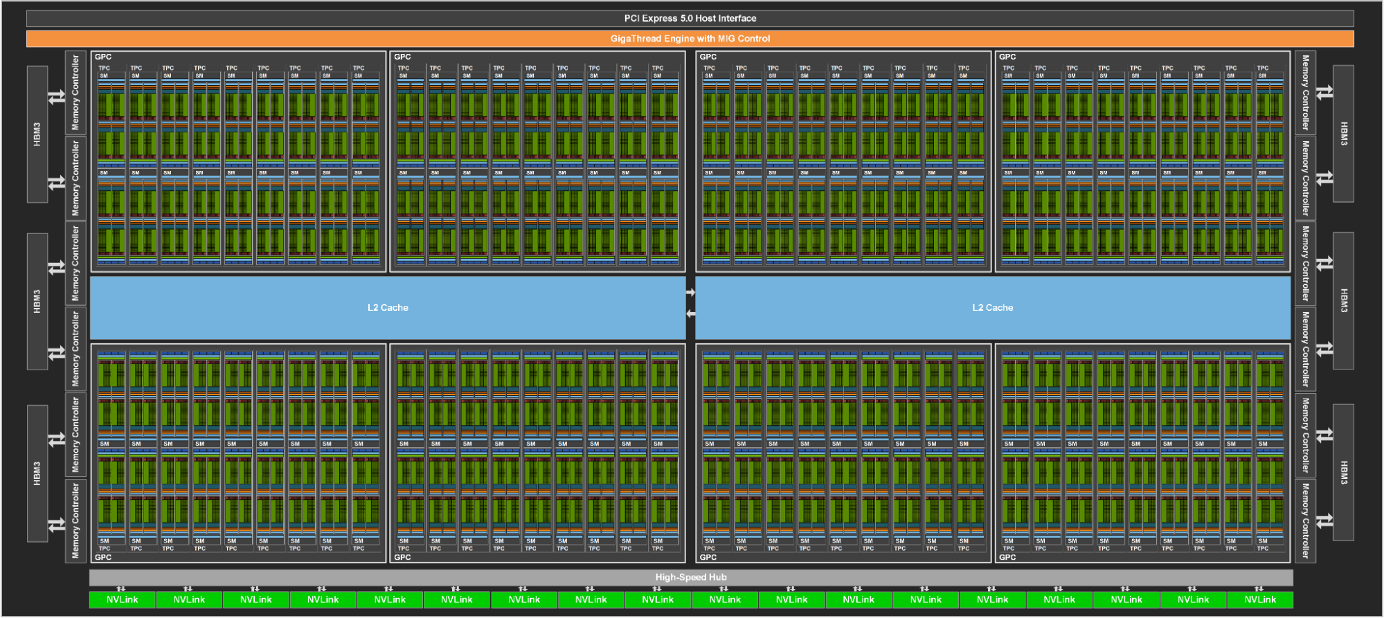
An SM (Streaming Multiprocessor) is the physical “workshop” of a GPU; a B200 has 148 SMs. A common misconception is to think of an SM as “one kind of core with multiple scheduling modes” — in reality, an SM contains five completely independent execution units, placed in parallel, sharing the same front-end control and the same register file and SMEM.
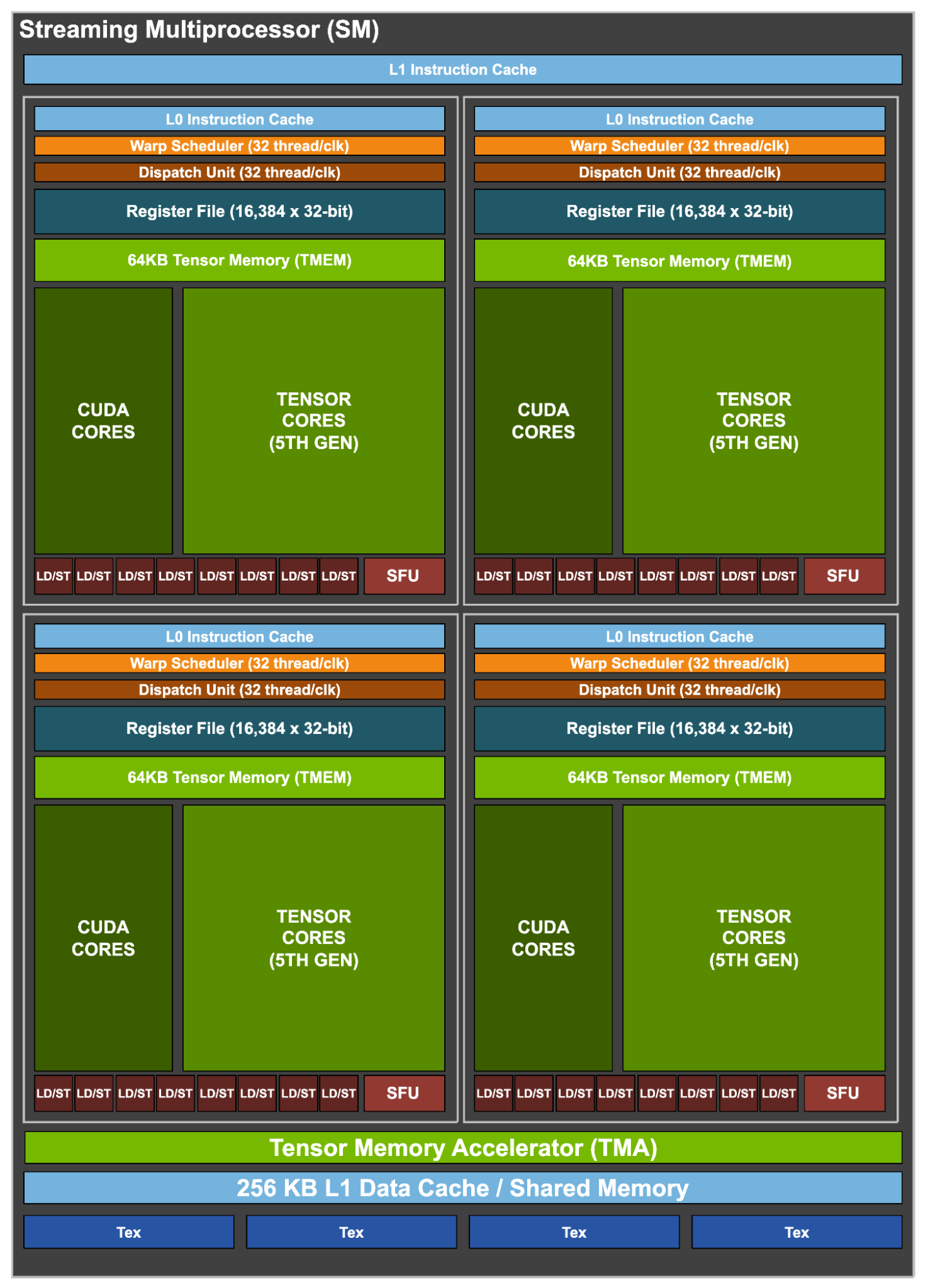
The most commonly misread part of this image is the parallel relationship between CUDA Cores and Tensor Cores. A common wrong model is “the Tensor Core internally coordinates multiple CUDA Cores to perform matmul” — this is wrong. The Tensor Core has its own dedicated, matmul-specialized silicon; in a B200 SM, the Tensor Core occupies more silicon area than the CUDA Cores. The straightforward counterexample: CUDA Core FP32 throughput is 80 TFLOPS, while Tensor Core FP16 throughput is 2250 TFLOPS — 28× higher. If Tensor Cores really were “implemented by orchestrating CUDA Cores,” where would this 28× come from?
How the Warp Scheduler Dispatches Instructions — Five Physically Independent Pipes · Shared Front-end
A more accurate framing is — the warp scheduler dispatches instructions to different pipes based on the instruction type: fma.f32 goes to the CUDA Core pipe, mma.sync to the Tensor Core pipe, ex2.f32 to the SFU pipe, ld.global to the LD/ST pipe, cuda::memcpy_async to the TMA pipe. The five pipes are physically completely independent, sharing only the front-end fetch, decode, and register file. This is structurally identical to how AVX units, scalar ALUs, and AES engines sit in parallel inside a CPU.
CUDA Core vs Tensor Core Circuit Differences — FMA Pipeline vs Systolic Array
Drill to the circuit level and the differences are not “size” — they are topology.
Scalar FMA Pipeline — CUDA Core’s Circuit
A CUDA Core is a scalar FMA unit: a 24×24-bit integer multiplier + a 24-bit adder + pipeline registers, around 20-30K transistors. Throughput is 1 FMA per cycle (= 2 floating-point ops). 128 CUDA Cores per SM are 128 independent FMA circuits placed in parallel, each working independently.
2D PE Array — Tensor Core’s Circuit
A Tensor Core is a 2D multiply-accumulator array, drawing on the core idea of systolic arrays. Data streams in by time step, each PE (Processing Element) performs a multiply-accumulate, and results either pass to neighbors or accumulate locally:
Why a Few-Hundred-× Gap — Three Physical Reasons
Why does this topology bring a few-hundred-× uplift? Three physical reasons:
- Maximize data reuse — a row of A entering the array flows through multiple PEs, reused N times, magnifying bandwidth by N. This is the physical foundation for exploiting matmul’s high arithmetic intensity.
- Eliminate control overhead — each FMA on a CUDA Core traverses warp scheduler → dispatch → register read → execute → writeback; control consumes 80%+ of the energy. The Tensor Core array is hardwired; one
mma.syncinstruction activates the whole array for several cycles with zero dynamic scheduling. - Local wires instead of global wires — wires between PEs in the array are short; wires between CUDA Cores must traverse the register file and are long. Short wires mean higher clock, lower power, smaller area.
NVIDIA in patents and papers deliberately avoids publicly admitting that Tensor Cores are textbook systolic arrays (Google TPUs do admit this); internally there are likely variants like adder trees mixed in. But this doesn’t affect the understanding — the critical insight is “lay down a hardwired MAC array”, not “a faster FMA.”
Circuit Difference Cheatsheet — Topology · Control · Programming Granularity
The table below nails down the circuit differences:
| Dimension | CUDA Core | Tensor Core |
|---|---|---|
| Circuit topology | scalar FMA + pipeline | 2D MAC array + hardwired data path |
| MAC count per operation | 1 | thousands to hundreds of thousands (growing each gen) |
| Control mode | dynamic scheduling (warp scheduler dispatches each instruction) | hardwired (one instruction activates the array for several cycles) |
| Programming granularity | each thread issues independently | 32-thread warp cooperative issue |
| Suited workloads | scalar / vector / control flow / activation functions | matmul / convolution |
| Silicon area share | ~30% | ~40% (B200 SM estimate) |
SFU / TMA / TMEM — Auxiliary Circuitry Built to Feed Tensor Cores
Tensor Core throughput grew so fast that it forced a sequence of supporting circuits. They don’t add FLOPS but ensure Tensor Cores “don’t starve” — and starvation is the number-one enemy of GPU optimization.
SFU — Transcendental Functions Hardwired
The SFU (Special Function Unit) handles transcendentals — sin / cos / exp / log / sqrt / rsqrt. The circuit is a small ROM (storing tens to thousands of sample points) plus a multiply-adder: the high bits of input x look up two samples, the low bits drive linear or quadratic interpolation, producing a result in a few cycles. This is tens of times faster than running a Taylor expansion on a CUDA Core. The cost is precision — __expf(x) via SFU gets about 8-9 significant bits; expf(x) in software has full 23 bits. The reason SFU count is small (4 per SM vs 128 CUDA Cores, ratio 1:32) is that it is pipelined: it can accept a new instruction every cycle, and 4 SFUs are enough to keep a warp’s transcendentals unblocked.
TMA — A Dedicated Unit for Async Tensor Movement
The TMA (Tensor Memory Accelerator) is a “tensor transfer specialist” introduced in Hopper. It addresses the problem that using LD/ST to move large tensors is wasteful: 32 threads of a warp each computing addresses, looping, and issuing loads has huge instruction overhead. TMA abstracts this into “tensor descriptor + one instruction”: you predefine a tensor map describing the tensor to move (multi-dim shape, stride, base address), then one thread issues a single instruction; the TMA hardware generates the address sequence, batches memory requests, writes into SMEM, and signals via async barrier when done. It is a small processor with a state machine, containing an AGU (Address Generation Unit), a request scheduler, and a layout transformer. Critically, TMA is asynchronous — the issuing thread returns immediately to do other work and re-synchronizes when data arrives. This unlocks the warp specialization pattern — a producer warp continually issues TMAs while a consumer warp continually drives Tensor Cores, fully overlapping the two.
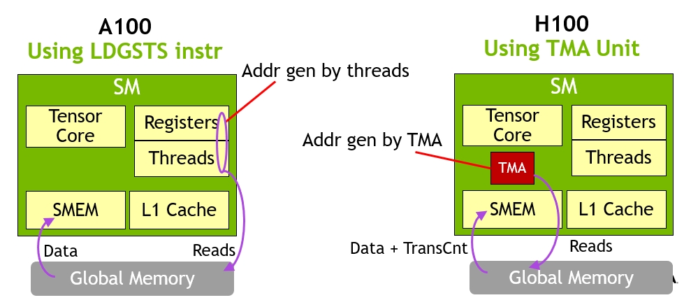
LDGSTS instruction to move tensors; each thread in a warp must compute an address and issue a load. Right: from Hopper H100 onward, a single thread issues one TMA instruction; the entire tensor is moved asynchronously to SMEM while the other threads simultaneously drive Tensor Cores. This is the physical basis of warp specialization.TMEM — Tensor Core Dedicated Accumulator Memory · Blackwell Onward
TMEM (Tensor Memory) appeared only in Blackwell — 256 KB of Tensor Core-dedicated SRAM bound inside the SM. It addresses a deeper bottleneck — when Tensor Core throughput hits multi-PFLOPS, even the register file can’t keep up. Before Hopper, mma operands and accumulators lived in the 32 threads’ registers; register-file port bandwidth became the bottleneck. Blackwell introduces TMEM: operands and accumulators sit in dedicated SRAM; the new tcgen05.mma instruction explicitly targets TMEM rather than registers, bypassing register ports entirely. This is why Blackwell can reach 80.7% of theoretical peak on FP64 GEMM (the equivalently sized H200 only reaches 55.6%).
| Unit | Role | Circuit essence | Generation introduced |
|---|---|---|---|
| SFU | transcendentals | ROM + interpolation multiply-adder | pre-Volta |
| TMA | async tensor transfer | AGU + state machine + layout transform | Hopper |
| TMEM | Tensor Core dedicated accumulator memory | independent SRAM + dedicated R/W ports | Blackwell |
These three together tell the same story — the stronger the Tensor Core, the more specialized auxiliary circuitry surrounds it. This is the physical embodiment of the “specialization ladder” growing narrower as you climb.
Memory Hierarchy — Explicit Management is the Essence of the GPU
Explicit vs Implicit Boundary — CPU Lets You Forget · GPU Forces You to Face
The GPU storage hierarchy is far more complex than the CPU’s, and the core difference is not “number of levels” but the boundary of “explicit” vs “implicit”. CPUs let you forget caches exist — write int x = arr[i] and hardware fetches automatically. GPUs force you to face them — write __shared__ float tile[256] to declare the buffer, then explicitly tile[tid] = gmem[idx] to move data, then __syncthreads() to wait.
Why Explicit Management Is Necessary — One SM Runs 2048 Threads
Why is explicit management necessary on a GPU? Because one SM concurrently runs 64 warps × 32 threads = 2048 threads; there is simply no way to give each thread its own cache and prefetcher. A CPU core serves one thread and can easily afford megabytes of cache; a GPU thread gets far fewer hardware resources per thread, so threads must explicitly organize data sharing among themselves — this is the fundamental reason SMEM must exist.
Management Mode Cheatsheet — Allocation · Movement · Access · Release
| Storage | Allocation | Data movement | Access | Release |
|---|---|---|---|---|
| Register | compiler-automatic | — | implicit | automatic |
| SMEM | programmer-declared | manual by programmer | implicit | automatic (at block end) |
| TMEM | programmer-explicit alloc | manual by programmer | via tcgen05 instructions | programmer dealloc |
| Constant | programmer-declared | one-time programmer fill | implicit | automatic |
| L1 / L2 | — | hardware-automatic | implicit | — |
| GMEM | cudaMalloc | cudaMemcpy | implicit | cudaFree |
| Other GPU HBM | NCCL allocates | NCCL/NVSHMEM | via API | NCCL releases |
The essence of GPU performance optimization is — keep data in the upper half of the hierarchy (registers / SMEM / TMEM / L2) and minimize trips back to HBM. Kernel fusion, FlashAttention, CUTLASS, warp specialization — all of these techniques boil down to this one objective.
Precision Evolution — FP4 Isn’t About Saving Money · It Treats One Chip as Four
Why Push Precision Down — More MACs Per Die
Mixed precision is the second main thread of this decade’s compute uplift — equal in stature to Tensor Core topology. Every generation introduces a lower precision, and the reason isn’t “cheaper” — it’s using the same silicon as multiple chips.
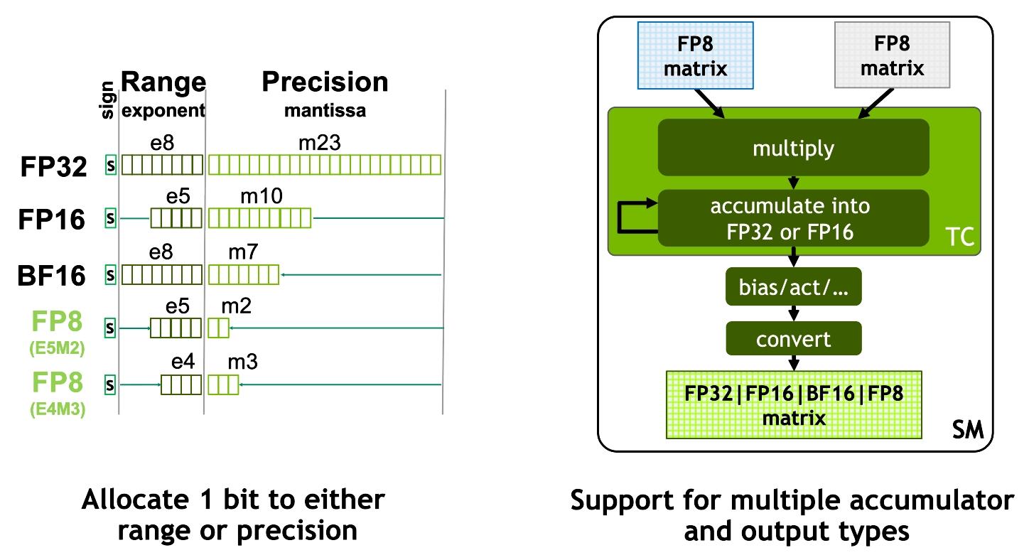
Physical Basis — Multiplier Area ∝ Width²
The underlying physical reason: multiplier area scales roughly with the square of bit width.
- FP32 multiplier: 24×24-bit integer multiplier (implicit 1 bit) → area unit 1
- FP16 multiplier: ~11×11 → area about 1/5
- FP8 multiplier: ~5×5 → area about 1/25
- FP4 multiplier: ~2×2 → area about 1/144
For the same silicon area, an FP4 multiplier fits 100× more units than FP32. Put differently — FP4 is not “cheap FP16,” it is “4× the MACs in the same silicon”.
Below is the Tensor Core throughput comparison across precisions on B200:
| Precision | Input width | Accumulator | B200 throughput | Relative to FP32 |
|---|---|---|---|---|
| FP32 (CUDA Core) | 32-bit | 32-bit | 80 TFLOPS | 1× |
| TF32 (Tensor Core) | 19-bit effective | 32-bit | ~1,100 TFLOPS | ~14× |
| FP16 / BF16 (Tensor Core) | 16-bit | 32-bit | 2,250 TFLOPS | 28× |
| FP8 (E4M3 / E5M2) | 8-bit | 32-bit | 4,500 TFLOPS | 56× |
| FP6 (E3M2 / E2M3) | 6-bit | 32-bit | ~6,750 TFLOPS | 84× |
| FP4 (E2M1) | 4-bit | FP32 or FP16 | 9,000 TFLOPS | 112× |
| FP4 + 2:4 sparsity | 4-bit | FP32 or FP16 | 18,000 TFLOPS | 225× |
| FP64 (Tensor Core) | 64-bit | 64-bit | 40 TFLOPS | 0.5× |
Note — Tensor Cores don’t only run low precision. They also support FP32 (via TF32 mode) and FP64 (for HPC). But low-precision throughput is far higher than high-precision, by deliberate trade-off, not capability limit.
Precision Added Per Generation — One Level Down Each Generation
The precisions added by each generation, mapped to hardware generations:
| Generation | Year | New precision | Main driver |
|---|---|---|---|
| Volta | 2017 | FP16 (Tensor Core first) | training |
| Turing | 2018 | INT8 / INT4 | inference quantization |
| Ampere | 2020 | TF32 / BF16 / 2:4 sparsity | training stability + free speedup |
| Hopper | 2022 | FP8 (E4M3 + E5M2) | LLM training + inference |
| Blackwell | 2024 | FP6 + FP4 + microscaling | LLM inference peak throughput |
| Rubin | 2026 | optimized FP4 + more microscaling | agent / reasoning inference |
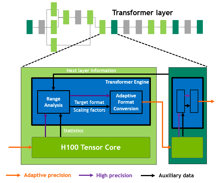
Every generation adds a new precision — but whether it’s usable is another matter. FP8 took two years from H100 release (2022) to production usability (2024), mainly via NVIDIA’s Transformer Engine library managing scaling factors automatically. FP4 is similar — hardware support is easy; numerical stability is the software task.
TF32 and Transformer Engine — Silent Speedups Without Code Changes
TF32 is a particularly elegant design. Its programmer-facing interface is FP32 (8-bit exponent + 24-bit mantissa, identical to IEEE FP32), but internally it truncates the mantissa to 10 bits (matching FP16) while preserving the 8-bit exponent. So the same cublasSgemm call — user changes nothing — automatically uses Tensor Cores for FP32 matmul, running ~14× faster than true FP32, with precision loss almost imperceptible for deep learning. This is NVIDIA’s clever way of letting Tensor Cores “silently take over all FP32 matmul.”
Deep Dive by Generation — Pascal · Volta · Turing · Ampere · Hopper · Blackwell · Rubin
Decompose the decade generation by generation, and each maps to a turning point in AI workloads:
Pascal · Volta · Turing — 2016-2018 · Tensor Core Era Begins
Pascal (2016, P100) — year one of data-center GPUs. First time abandoning GDDR for HBM2 (720 GB/s), first introduction of NVLink (160 GB/s, ~5× PCIe), first native FP16 (on CUDA Cores, 2× FP32 throughput). No Tensor Core yet. This generation proved the commercial viability of “GPUs in the data center training deep learning.” Most GPT-2 / BERT-era training ran on P100s.
Volta (2017, V100) — Tensor Core era begins. First-gen Tensor Cores, 8 per SM, performing 4×4×4 FP16 matmul, delivering 12× training speedup. This was the fundamental shift in GPU design philosophy — from “general-purpose parallel compute chip” to “AI chip purpose-built for matmul acceleration.” From this generation onward, per-generation compute gains come mainly from Tensor Cores, not CUDA Cores. The earliest GPT-3 was trained on V100 clusters.
Turing (2018, T4 + RTX 20) — inference market diverges. T4 is low-power (70W), introduces INT8 Tensor Cores, targets inference serving; the same-generation consumer RTX 20 series introduces RT Cores (ray tracing hardware). Proved viability of the “V100 for training, T4 for inference” differentiation strategy.
Ampere · Hopper — 2020-2022 · Industrializing LLM Training
Ampere (2020, A100) — industrializing LLM training. Third-gen Tensor Cores introduced TF32 (auto-speedup for vast amounts of FP32 code with hardly any changes), BF16 (wider numerical range, more stable training), and 2:4 structured sparsity (another 2× throughput). Added MIG (slice one A100 into 7 small GPUs), second-gen NVLink (600 GB/s), HBM2e. A100 is NVIDIA’s most durable card — still serving in large numbers across data centers in 2026.
Hopper (2022, H100) — Transformer specialization. Fourth-gen Tensor Cores + the Transformer Engine software layer = native FP8 + automatic quantization for the first time. Introduced TMA to solve “Tensor Core is too fast, registers can’t keep up,” and Thread Block Cluster to let multiple SMs cooperate (8 blocks per cluster sharing distributed SMEM). NVLink 3 (900 GB/s) + HBM3 (3 TB/s). H100 is 6-9× faster than A100 on Transformer training. Grace-Hopper Superchip (GH200) for the first time tightly couples CPU and GPU via NVLink-C2C.
Blackwell · Rubin — 2024-2026 · Multi-die + FP4 + Platform
Blackwell (2024, B200) — multi-die + FP4 era. First dual-die design — two reticle-limit dies connected by 10 TB/s internal interconnect, presenting to software as a single GPU, totaling 208 B transistors. Fifth-gen Tensor Cores natively support FP4 / FP6, paired with second-gen Transformer Engine’s micro-tensor scaling. Introduced TMEM (256 KB Tensor Core dedicated SRAM), 2-CTA Cluster (two SMs jointly feeding one Tensor Core UMMA), and decompression engines (LZ4/Snappy/Deflate, for data analytics). NVLink 5 (1.8 TB/s) + HBM3e (8 TB/s, 192 GB). GB200 NVL72 integrates 72 B200s + 36 Grace CPUs into a single rack.
Rubin (2026, R100) — platform era. 336 B transistors, a truly multi-die design (two compute dies + two I/O dies). HBM4 (288 GB, 22 TB/s bandwidth, ~2.8× B200). 224 SMs/GPU, FP4 throughput 50 PFLOPS (sparse). NVLink 6 (3.6 TB/s/GPU). The most important shift is philosophical — NVIDIA no longer sells GPUs but an entire rack-scale AI compute platform; the Vera Rubin platform is organized around “seven-chip co-design” (R100 GPU + Vera CPU + NVLink 6 Switch + ConnectX-9 + BlueField-4 + Spectrum-6 + an integrated Groq 3 LPU).
Ten-Year Main Threads — Precision · Array · Storage · Interconnect · Business Form
In a single table, the main threads of the decade are crystal clear:
| Thread | Manifestation |
|---|---|
| Precision shrink | FP16 → INT8 → BF16 → FP8 → FP4, one added each gen |
| Tensor Core array size | 4×4×4 → 16×16×16 → 64×8×16 → 128×256×16 |
| On-die storage made explicit | SMEM expanded → cp.async → TMA → Cluster → distributed SMEM → TMEM |
| Exponential interconnect growth | NVLink 160 GB/s → 3600 GB/s · HBM 720 GB/s → 22 TB/s |
| Business form | sell GPUs → sell DGX → sell racks → sell AI factories |
CUDA Cores are nearly absent from this table — their FP32 throughput went from 10.6 to 100 TFLOPS, only 10× in a decade. General compute ceding ground to specialized compute is the most direct conclusion of the decade.
Programming Model Expansion — Thread → Warp → Block → Cluster → Grid
From Three Tiers to Five — Warp and Cluster Inserted in the Middle
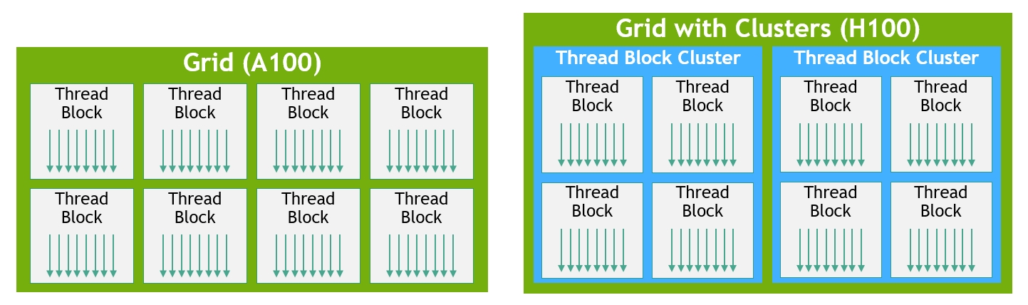
As hardware complexity rose, the programmer-facing programming model expanded with it. The classic CUDA model is three tiers — Thread / Block / Grid: each thread is independent, threads inside a block share SMEM, and the Grid is all blocks. But after the Tensor Core era, Warp and Cluster were forcibly inserted in the middle, making it five:
Why Warp Must Become Explicit — mma.sync Is Physically a Warp-Level Instruction
Why did the Tensor Core era have to make warps explicit? Because the mma.sync instruction is physically warp-level — 32 threads must cooperatively issue it; elements of matrices A and B are distributed across the registers of these 32 threads in a specific layout, and the Tensor Core hardware gathers all threads’ register contents to feed the array. A 16×16×16 matmul needs 512 FP16 inputs = 1024 bytes, which doesn’t fit in a single thread’s registers — it must be spread across 32 threads. So the programmer must upgrade from “what does my thread compute” to “what does our warp jointly compute”.
Cluster’s Introduction Rationale — Multiple SMs Jointly Feed One mma
Cluster follows the same logic — Hopper-era Tensor Core throughput grew to need multiple SMs feeding data, so clusters were introduced so that blocks in a GPC share SMEM (distributed SMEM) and TMA. Blackwell’s 2-CTA cluster further binds two SMs into a group to jointly feed one UMMA Tensor Core instruction.
Code Comparison — naive matmul → wmma → wgmma+TMA → tcgen05+TMEM
The most direct experience is to see how the same task (matmul) evolves across generations. The four code snippets below show the typical matmul shape for Pascal → Volta-Ampere → Hopper → Blackwell.
Pascal · Naive Thread Level — Each Thread Computes One Element
__global__ void matmul_naive(float* A, float* B, float* C, int N) {
    int row = blockIdx.y * blockDim.y + threadIdx.y;
    int col = blockIdx.x * blockDim.x + threadIdx.x;
    if (row >= N || col >= N) return;

    float sum = 0;
    for (int k = 0; k < N; k++) {
        sum += A[row * N + k] * B[k * N + col];
    }
    C[row * N + col] = sum;
}
Thinking granularity: single thread. Each thread computes one element of C, looping N times for the inner product. Code readability is high — but performance is only 5-10% of theoretical peak (no Tensor Core, data loaded directly from GMEM).
Volta–Ampere · wmma Fragment — Warp Cooperation · First Tensor Core
#include <mma.h>
using namespace nvcuda::wmma;

__global__ void matmul_wmma(half* A, half* B, float* C, int N) {
    __shared__ half tile_A[16][16];
    __shared__ half tile_B[16][16];

    // fragments live in the registers of all 32 threads in the warp
    fragment<matrix_a, 16, 16, 16, half, row_major> a_frag;
    fragment<matrix_b, 16, 16, 16, half, col_major> b_frag;
    fragment<accumulator, 16, 16, 16, float> c_frag;
    fill_fragment(c_frag, 0.0f);

    for (int k = 0; k < N; k += 16) {
        // Async load into SMEM (cp.async from Ampere)
        // ... loading logic omitted ...
        __syncthreads();

        load_matrix_sync(a_frag, &tile_A[0][0], 16);   // warp-cooperative
        load_matrix_sync(b_frag, &tile_B[0][0], 16);

        mma_sync(c_frag, a_frag, b_frag, c_frag);      // one instruction = 16×16×16 matmul
        __syncthreads();
    }

    store_matrix_sync(&C[...], c_frag, N, mem_row_major);
}
Thinking granularity upgrades to the whole warp. Note several key changes — every wmma API ends with _sync, meaning “the whole warp must call and execute it synchronously”; the code has no threadIdx — fragments hide the thread-level complexity; mixed precision appears for the first time (input half, accumulator float). Performance can reach 60-80% of peak.
Hopper · TMA + Warp Specialization — Producer / Consumer Pipelined Overlap
// Extremely simplified — real CUTLASS code is several times longer
__global__ void matmul_hopper(...) {
    __shared__ AsyncBarrier bar;
    extern __shared__ half smem_buffer[];

    int warpId = threadIdx.x / 32;

    if (warpId == 0) {
        // Producer warp — issues TMA loads only, no compute
        for (int k = 0; k < N; k += TILE_K) {
            cuda::memcpy_async(smem_A, gmem_A_tile, tma_desc_A, bar);
            cuda::memcpy_async(smem_B, gmem_B_tile, tma_desc_B, bar);
            bar.arrive();
        }
    } else {
        // Consumer warps — drive Tensor Cores, no loads
        for (int k = 0; k < N; k += TILE_K) {
            bar.wait();                                   // wait for data arrival
            wgmma::mma_async(c_frag, smem_A, smem_B);     // async mma!
            wgmma::commit_group();
            wgmma::wait_group<0>();
        }
    }
}
Thinking granularity upgrades again — warp specialization. Different warps do completely different work — some only move data (producer), some only drive Tensor Cores (consumer); the two pipes synchronize via async barrier. wgmma (warpgroup MMA) replaces wmma; operands can come directly from SMEM rather than first being loaded into registers. Async barriers don’t count threads — they count bytes — “I wait for 16 KB of data to land.” Performance reaches 85-95% of peak, but such code is essentially writable only by CUTLASS / FlashAttention teams.
Blackwell · tcgen05 + TMEM — 2-CTA Cluster · Operands Bypass Registers
__global__ void matmul_blackwell(...) {
    // Explicit TMEM allocation
    auto tmem_c = tcgen05::alloc<float, 128>();
    __shared__ AsyncBarrier bar;

    if (in_producer_warp) {
        // TMA multicast — one load, both SMs in the 2-CTA cluster receive
        cuda::memcpy_async_tma_multicast(smem_A, gmem_A, cluster);
        cuda::memcpy_async_tma_multicast(smem_B, gmem_B, cluster);
    } else {
        // Operands come from SMEM, result writes into TMEM (no register pressure)
        tcgen05::mma(tmem_c, smem_A, smem_B);
        tcgen05::commit();
    }

    // Read result out of TMEM
    tcgen05::load(c_reg, tmem_c);
    tcgen05::dealloc(tmem_c);
}
Another manual-management layer is added — explicit TMEM alloc / dealloc. The tcgen05.mma instruction takes operands from SMEM and stores accumulators in TMEM, fully bypassing the register file. The 2-CTA cluster lets two adjacent SMs share data via distributed SMEM + TMA multicast and jointly feed one mma. A single activation of the cluster does an enormous amount of work.
Per-Generation Complexity Comparison — Each Generation 2-3× More Code
Put the four snippets together and the evolution is plain:
| Generation | Thinking granularity | New things the programmer must manage | Code volume |
|---|---|---|---|
| Pre-Pascal | Thread | thread / block / grid trio | ~20 lines |
| Ampere | + Warp | fragment layout / _sync semantics / cp.async | ~100 lines |
| Hopper | + Cluster | TMA descriptors / warp specialization / async barrier | ~300 lines |
| Blackwell | (Cluster upgrade) | TMEM alloc/dealloc / tcgen05 / 2-CTA / multicast | ~500 lines |
Each generation roughly 2-3× more complexity. But this is only the bare-CUDA perspective — in the real world, 90% of users don’t write this kind of code.
Abstraction Layers Absorb the Complexity — torch.matmul Doesn’t Change · cuBLAS Is Rewritten Each Gen
Code Volumes Across Five User Tiers — From 1 Line to 1000 Lines of Assembly
This is the essence of NVIDIA’s design philosophy — hardware complexity exploded, absorbed by layered abstractions, while the regular user’s experience stayed stable or even simpler.
For the same matmul task, the code volume across user groups:
| User group | Invocation | Code volume | Performance | What you must know |
|---|---|---|---|---|
| Regular AI engineer | torch.matmul(a, b) | 1 line | near peak | almost nothing |
| Custom kernel engineer | Triton @triton.jit + tl.dot | ~50 lines Python | 80-95% peak | tile partitioning / SMEM concept |
| High-performance library developer | CUTLASS templates | ~100 lines C++ | near peak | Tensor Core / CuTe layout |
| Bare-CUDA engineer | direct mma.sync | ~300 lines C++ | depends on skill | warp / SMEM banks / mma instructions |
| Extreme optimizer | inline PTX | ~1000 lines assembly | theoretical limit | register allocation / instruction scheduling / dependency tracking |
The further down, the more control, but the work explodes. FlashAttention’s author Tri Dao writes at the bare-CUDA + inline PTX level, so one person can write some kernels faster than the cuBLAS team. But the vast majority of AI engineers stay at the top tier.
Why Hand-Written Code Isn’t Always Faster Than cuBLAS — NVIDIA’s Moat Is More Than Hardware
An interesting reversal — 90% of the time, PyTorch + cuBLAS beats a typical engineer’s hand-written CUDA by a wide margin. Three reasons:
- cuBLAS is tuned by NVIDIA engineers per generation; they know every detail of Tensor Cores (including undocumented ones).
- cuBLAS internally is a kernel library — for the same matmul, dozens of kernel implementations exist, and at runtime the optimal one is auto-picked by shape.
- Optimizations few would think of — double buffering, warp specialization, bank-conflict avoidance, register pressure balancing.
So NVIDIA’s moat is not just the hardware, it’s this whole top-to-bottom software stack. This is also why AMD GPUs can numerically catch up to or even surpass NVIDIA, but the ecosystem is far behind — hardware can be matched; the libraries and compilers accumulated over the past decade-plus cannot.
Software Stack and Open-Source Landscape — Open Shell · Closed Core
CUDA Software Stack in Layers — L7 Frameworks → L1 Hardware · A Seven-Tier Slice
Draw the CUDA library ecosystem accumulated over a decade-plus, and a counterintuitive truth emerges — the most central and most used libraries are precisely the closed-source ones, while open-source ones are upper, peripheral, or customization-facing.
Open vs Closed Boundary — The Most-Used Libraries Are Precisely Closed
Many people mistakenly assume cuBLAS and cuDNN are open source — in fact they are NVIDIA’s most tightly guarded products. pip install nvidia-cublas-cu12 installs not source code but precompiled .so binaries; the license field clearly states LicenseRef-NVIDIA-Proprietary.
| Library | Open-source status | License | What you can see |
|---|---|---|---|
| CUDA Runtime / Driver | closed | NVIDIA Proprietary | only headers and .so |
| cuBLAS / cuBLASLt | closed | NVIDIA Proprietary | only headers and .so |
| cuDNN (core) | closed | NVIDIA Proprietary | only headers and .so |
| cuDNN Frontend (C++ wrapper) | open | MIT | wrapper, calls closed cuDNN |
| cuFFT / cuSPARSE / cuSOLVER | closed | NVIDIA Proprietary | only headers and .so |
| CUTLASS | fully open | BSD-3-Clause | full C++ template source |
| Triton (OpenAI) | fully open | MIT | full source |
| NCCL | fully open | BSD-3 | full source |
| NVSHMEM (post-2024) | open | BSD-3 | full source |
| Transformer Engine | fully open | Apache 2.0 | full source |
| TensorRT | partial | Apache 2.0 (plugins) | only plugins, parsers; core closed |
| TensorRT-LLM | partial | Apache 2.0 (frontend) | frontend Python, depends on closed TensorRT |
| RAPIDS (cuDF / cuML) | fully open | Apache 2.0 | full source |
| Megatron-Core / NeMo | fully open | Apache 2.0 | full source |
The Real Moat — Not a Single Library · The Decade-Plus Ecosystem
NVIDIA pursues an “open shell + closed core” product strategy: users can extend (write custom plugins, modify CUTLASS templates, customize NCCL communications) but cannot copy the core implementations. Even if AMD ROCm open-sources the equivalent libraries (rocBLAS / MIOpen are both open), performance still trails cuBLAS / cuDNN by 2-3 years — because the optimization tricks of cuBLAS / cuDNN (the latest Tensor Core instructions, warp scheduling, TMA usage) live in the binary, and AMD can’t “copy” them — only reverse-engineer or reinvent them.
This is NVIDIA’s true moat — not any single library, but dozens of libraries layered over a decade-plus.
Summary — Scale Tensor Cores · Scale Precision · Scale Abstraction Layers
Three Main Threads — Tensor Core · Precision · Abstraction
Compressing the decade into one sentence: NVIDIA did three things this decade — scale Tensor Cores, scale mixed precision, scale abstraction layers to absorb complexity.
Specifically:
- Scale Tensor Cores — essentially all compute gains come from here. On a B200, Tensor Core throughput is ~60-250× CUDA Core. It is not a faster CUDA Core; it is a completely different systolic-like array.
- Scale precision — push one level down each generation. FP32 → TF32 → FP16/BF16 → FP8 → FP4. Each step packs 4× more MACs into the same silicon, doubling LLM inference throughput for free.
- Scale abstraction layers —
torch.matmul(a, b)doesn’t change a single character, while cuBLAS / cuDNN gets rewritten each generation. CUTLASS / Triton / Transformer Engine absorb hardware complexity, letting users stay at the “PyTorch is enough” experience.
Why Tensor Cores — Physical · Architectural · Commercial
If you ask “why Tensor Cores instead of CUDA Cores,” the answer lives at three layers:
- Physical layer — CUDA Cores are near frequency limits; piling on SMs is constrained by power and thermals; Tensor Cores still have two open paths: precision shrink and array scale.
- Architectural layer — Tensor Cores’ hardwired control makes control overhead nearly zero; effective compute per silicon area is much higher.
- Commercial layer — Tensor Cores + closed cuBLAS / cuDNN are NVIDIA’s true moat; no matter how fast AMD hardware gets, it can’t replicate this software stack.
Five-Year Outlook — FP2 · Larger Clusters · Platformization
The trajectory continues for the next 5 years — Rubin Ultra (2027) / Feynman (2028) are already on the roadmap, FP2 / INT2 may appear in the generation after that, clusters may scale from 8-16 blocks to dozens, TMEM may further specialize into more dedicated storages. For you, once you grasp this main thread, any future NVIDIA news, architecture, or product can be located immediately: it’ll be one more notch on one of “scale Tensor Cores / scale precision / scale abstraction layers.”
References — Whitepapers · Papers · Docs
Whitepapers and Official Documentation
- NVIDIA Architecture Whitepapers — each release ships with a very detailed Architecture Whitepaper; this is the most authoritative primary source. At minimum read the Hopper and Blackwell whitepapers.
- CUDA C++ Programming Guide — official handbook; chapter 3 on async copy, chapter 5 on Tensor Cores, chapter 7 on clusters give the concrete syntax of the model’s expansion.
- CUTLASS GitHub — the latest CUTLASS 4.x + CuTe DSL is the most authoritative open-source implementation pushing every architectural feature to its limit. github.com/NVIDIA/cutlass
Papers and Engineering Blogs
- Tri Dao’s FlashAttention papers — FlashAttention (2022) / FA-2 (2023) / FA-3 (2024). Canonical example of stringing TMA + warp specialization + Tensor Cores; FA-3 exploits nearly every Hopper feature.
- Colfax Research TMA / wgmma tutorials — the clearest engineering-level walkthrough of Hopper’s TMA, wgmma, and async barriers.
- Aleksa Gordić’s “matmul anatomy” blog — step-by-step derivation from a naive matmul to a CUTLASS-style kernel; one of the best continuous reads from beginner to advanced.
Textbooks and Courses
- “Programming Massively Parallel Processors” (Kirk & Hwu) — GPU parallel programming textbook covering hardware, CUDA, and distribution. From the 5th edition onward, it added much Volta-Ampere era content.
- CMU 15-418 / Stanford CS149 — lecture notes and assignments from both are public, covering parallel architectures, SIMT, and memory models more clearly than most books.